 | –≠–ª–µ–∫—Ç—Ä–æ–Ω–Ω—ã–π –∫–æ–º–ø–æ–Ω–µ–Ω—Ç: AK5393 | –°–∫–∞—á–∞—Ç—å:  PDF PDF  ZIP ZIP |

ASAHI KASEI
[AKD5393 Rev.A]
<KM059101>
'00/05
- 1 -
General description
The AKD5393 is an evaluation board for the AK5393 professional audio 24bit A/D converter. The
AKD5393 includes the input buffer circuit and also has a digital interface transmitter. Further, the
AKD5393 can evaluate direct interface with AKM's DAC evaluation boards.
n
Ordering guide
AKD5393 Rev.A --- Evaluation board for AK5393VS
Function
∑
On-board Full-differential input buffer circuit
∑
On-board clock generator
∑
Compatible with 2 types of interface
1) Direct interface with AKM's DAC evaluation boards.
2) On-board CS8402 as DIT which transmits optical output.
∑
A BNC connector for an external clock input.
* Circuit diagram and PCB layout are attached at the end of this manual.
Evaluation board Rev.A for AK5393
AKD5393
Input
Buffer
AK5393
Clock
Generator
D/A Data
10pin Header
Lch
Rch
+5V GND
CS8402
(DIT)
Opt Out
-15V
+3.3V
+15V

ASAHI KASEI
[AKD5393 Rev.A]
<KM059101>
'00/05
- 2 -
n
Input buffer circuit
The AKD5393 includes full-differential input buffer circuit with an inverted-amp (gain: -10dB). The capacitor of 10nF
between AIN+ /- decreases the clock feed through noise of modulator, and composes a 1st order LPF (fc=360kHz) with
22ohm resistor before the capacitor. This circuit also has a 1st order LPF (fc=370kHz) composed of op-amp. External
analog signal can be fed through the BNC connector or the Cannon connector.
4.7k
-
+
-
+
22
3k
910
-
+
22
910
AK5393
AIN+
AIN-
CAL
ZCAL
Analog In
8.1Vpp
"L" at self calibration
47
µ
47
µ
NJM5532
VA=
±
5V
VP=
±
15V
4.7k
10
µ
+
10k
10k
0.1
µ
Bias
VA+
2.45Vpp
2.45Vpp
VP+
VP-
Bias
470p
3k
470p
Bias
10n
Figure 1. Full-differential input buffer circuit example
1: In case of using the BNC connector
[JP2, JP3, JP4, JP5]: Short
[R11, R18]:
Open
The resistor value of R10 and R19 should be properly selected in order to much the output
impedance of the signal source.
2: In case of using the Cannon connector
[JP2, JP3, JP4, JP5]:
Open
The resistor value of R10, R11, R18 and R19 should be properly selected in order to much the
output impedance of the signal source.
* AKM assumes no responsibility for the trouble when using the above circuit examples.
n
Power supply and Decoupling
VA and VD supplies to the AK5393 are decoupled separately in order to minimize the effect of the digital noise. A system
analog supply is fed to VA. VA and VD lines should be distributed separately from the power unit.
Decoupling capacitors are connected to AK5393 as near as possible, particularly the ceramic capacitor to the VREFL/R
pin.

ASAHI KASEI
[AKD5393 Rev.A]
<KM059101>
'00/05
- 3 -
n
Operation sequence
(1) Set up the power supply lines
VP+=+15V, VP- = -15V, VA+=+5V, VD+=+3.3V
5.25V, AGND=DGND=0V
Each supply line should be distributed from the power unit.
(2) Set up the evaluation modes and jumper pins. (See next item)
There are many jumper pins to cover many evaluation modes.
Please take care of setting.
(3) Set up the DIP SW position for the DIT. (See next item)
This does not affect AK5393 operation.
(4) Power On.
The AK5393 should be reset once by bringing PD "L"(SW4) upon power-up.
(5) AK5393 can be reset by SW4 during operation.
Lower position resets the device, and the upper position is for normal operation.
Note: In any case of changing clocks during operation, the device should be reset by
bringing PD "L". If not followed, the AK5393 may be destroyed since its internal logic
uses dynamic circuit.
n
The evaluation modes and corresponding jumper pin settings.
1. Evaluation Mode
Applicable Evaluation Mode
1-1 Using D/A converter board for the analog performance analysis.
1-2 DIT (Optical Link) [Default]
1-3 All interface signals (MCLK, BICK and LRCK) are fed from external circuit.
1-4 Feed all interface signals to the external circuit through PORT2.
1-1. Using D/A converter board for the analog performance analysis.
The AK5393 can be evaluated by distortion analyzer using various AKM's D/A converter evaluation boards
through PORT2.
[Slave mode]
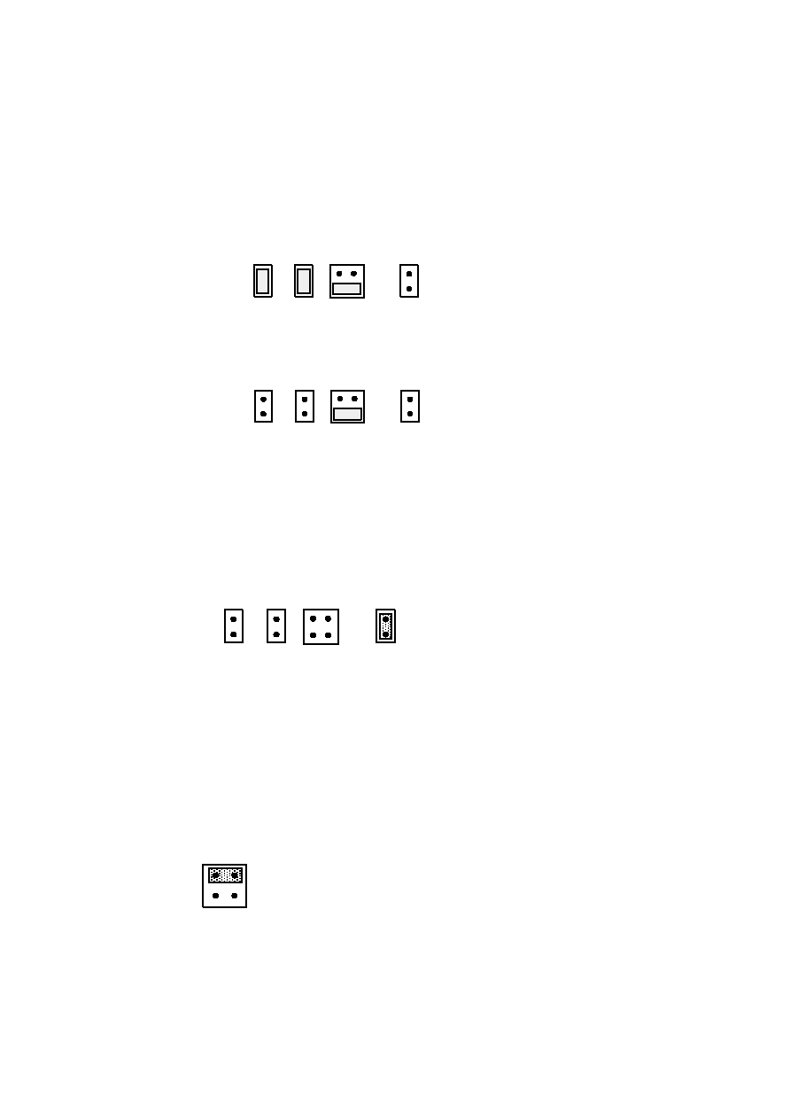
Figure 2. Jumper set up (D/A)
JP9
LR
JP7
BC
JP11
MCLK
EXT
XTL
JP12
XTE
ASAHI KASEI
[AKD5393 Rev.A]
<KM059101>
'00/05
- 4 -
1-2DIT (Optical Link)
PORT1 is used. DIT generates audio Bi-phase signal from received data and which is output through optical
connector (TOTX174). It is possible to connect AKM's D/A converter evaluation boards on the digital-amplifier,
which equips DIR input. There are two kinds of jumper setting depend on the SMODE1 and SMODE2 pin. The
interface signals are output from PORT2. (See the (4)). In case of using external clock through a BNC connector,
select EXT on JP11 (MCLK) and short JP12 (XTE).
[Slave mode] (Default)
[Master mode]
Figure 3. Jumper set up (DIT)
1-3 All interface signals (MCLK, BICK and LRCK) are fed from external circuit. [Slave mode]
Under the following setup, MCLK, LRCK and SCLK signals needed for the A/D to operate could be
Fed through PORT2.
Figure 4. Jumper set up (EXT)
1-4 Feed all interface signals to the external circuit through PORT2.
[Master, Slave mode]
Please set up as same as 1-2. All interfacing signal which drive AK5393 are output through PORT2.
However, the FSYNC signal is input when the position of the SDATA is needed to be controlled.
* Setting for double speed sampling (fs=96kHz)
For the double speed sampling, DFS="L", MCLK=128fs, BICK=64fs(max) are required.
So, when BICK and LRCK are created from 74HC4040 on the board, the crystal oscillator should be changed to
24.576MHz and set JP14 (MCLK2) to 128fs side (see the schematics).
2. BIT CLK (BCF) set up
[JP8] Either 64fs or 128fs for the BCF can be selected. Figure shows 128fs example.
When DFS="H", set JP8 to 64 side.
128:
128fs is fed to AK5393 as BICK.
64:
64fs is fed to AK5393 as BICK.
JP9
JP7
BC
JP11
MCLK
EXT
XTL
JP12
XTE
LR
JP8
64
128
BCF
JP9
JP7
BC
JP11
MCLK
EXT
XTL
JP12
XTE
LR
JP9
JP7
BC
JP11
MCLK
EXT
XTL
JP12
XTE
LR

ASAHI KASEI
[AKD5393 Rev.A]
<KM059101>
'00/05
- 5 -
3. Jumper-set up and explanation
Set up the CS8402's data format corresponding the serial data interface of the AK5393.
AKD5393
Data Format
SMODE2
(SW2-5)
SMODE1
(SW2-4)
8402
(SW2-1)
BCF
(JP6)
LRP
(JP10)
Slave mode
ON
ON
ON
F
H
Mater mode
ON
OFF
OFF
R
L
I
2
S Slave mode
OFF
ON
OFF
R
H
I
2
S master mode
OFF
OFF
OFF
R
H
*DIP-SW is ON="L"
OFF="H"
Table 1. Serial data interface of AK5393 and CS8402
[SW2-1]: CS8402's data format
ON: MSB justified, 24bit
OFF: IIS Compatible
[JP6] : Define the polarity of SCLK.
F: SCLK is inverted.
R: SCLK coincides with AK5393
[JP10]: Define the polarity of LRCK.
L: LRCK is inverted.
H: LRCK coincides with AK5393.
4. The other function set up
No.
PIN
ON
OFF
1
8402
See the Table1.
2
DFS
48k
96k
3
HPFE
disable
enable
4
SM1
5
SM2
Seethe Table 1.
6
CALMODE
VCOM
AIN
*DIP-SW is ON="L" OFF="H"
Selects the sampling rate.
Selects HPF of AK5393.
Selects the reference signal for Offset-Cal of K5383
Table 2. DIP-SW2 set-up
VCOM:VCOML,VCOMR pin
AIN: Analog input pin (AINL
±
, AINR
±
)
[JP13]: Selects the analog power supply source to VA pin of the AK5393.
Open: Supply from the power supply terminal (VA+).
Short: Supply from 3-terminal-voltage regulator (+5V) on the board.
n
The function of the toggle SW.
[SW3] Resets the CS8402. Upper position resets the internal counter of CS8402, then Bi-phase
signal is not output. Keep the "L" position during normal operation.
[SW4] Resets the AK5393. Keep the "H" position during conversion.